"Let there be MEMS"...
On the 29th December 1959, Richard Feynman, future Nobel Prize winner, gave a talk at the meeting of the American Physical Society entitled: There is plenty of room at the bottom . In his talk he proposed that many different end applications could come from the ability to manipulate matter at the nano-metric scale. As a theoretician, Feynmann did not know how to achieve this; however he correctly anticipated many possible applications. His talk was given at a time when current processes for fabricating microelectronic chips had not been invented, however it did not prevent his vision of the future. He concluded that, if we could manipulate atoms, we could write the equivalent of the Encyclopaedia Britannica on the head of a pin. Chemistry would also be a matter of single atom manipulation rather than complex chemical reactions. We could build wires and tools at the microscopic scale, atom by atom.
He finished his talk with two challenges: to build a tiny working electric motor that would fit inside a cube of 6-mm on each side and to write the information from a book page on a surface area 25000 times smaller than its standard print (a scale at which the entire contents of the Encyclopedia Britannica could fit on the head of a pin). He offered prizes of $1000 for each challenge. A year later, William McLellan, a meticulous craftsman, achieved a 250-microgram 2000-rpm motor; he succesfully met Feynman's challenge using only conventional tools. However it is only much later in 1985 that Tom Newman claimed the second challenge. He successfully reduced the first paragraph of A Tale of Two Cities by 1/25000, and collected the second Feynman prize.
MEMS became practical once they could be fabricated using modified semiconductor device fabrication technologies, normally used to make electronics.
|
|
|
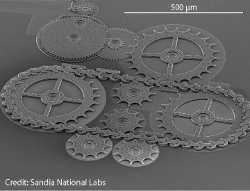
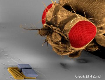
Some examples of MEMS devices (Credit: Sandia National Labs and ETH Zurich)
“Imagine a machine so small that it is invisible to the naked eye. Imagine those machines with gears not much bigger than a grain of pollen. Imagine those machines manufactured by thousands at the same time at a cost of a few tenths of euros each. Imagine a world so small that gravity has no importance but where atomic forces prevail…” (Paul McWhorter).
Thermoelectric based MEMS sensors
My involvement in MEMS sensors dates from the time of my M.Sc. where I used to work on a thermoelectric micro-converter based on Seebeck and Peltier effect.
The laboratory I was working for (CEM2 – Montpellier University, France) was developing a nice sensor based on the two effects. The device was a thermopile, it consisted in a thermocouple below which a micro-Peltier-module was used to cool down the sensing surface; having the sensing surface at constant temperature allowed better sensitivity and response from the sensor.
The same device was also used as a vacuum sensor. The Peltier module was this time used as a heater; the temperature measurement via the thermocouple was highly dependent on the vacuum level (particle concentration in the surrounding medium).
You would have guessed that being my first experience in the micro-sensor field my contribution to the development of the sensor was a bit limited. However, on top of being in charge of the device characterization I have successfully proposed an electronic architecture for the sensor. The aim was to have a closed-loop control of the temperature of the sensing surface (the Peltier part of the device) and a conditioning and processing of the output of the sensor. I left the project with the proposed electronics at the simulation stage (validated with P-Spice).
Test of MEMS
An important side of designing sensor devices especially MEMS is the ability to test them prior to packaging. Packaging of MEMS device can count for approximately 30% of the total cost of the solution. This is due to the fact that MEMS sensors need to communicate with the outer-world and dedicated packaging is required. A lot of effort is undertaken to avoid spending time and money packaging faulty devices. The challenge here is to provide a proper stimulus that will tell if the device is faulty knowing that the device is not packaged yet (we are talking here of devices at the wafer stage) and sometimes physical stimuli stresses can’t be applied. For instance if you want to test an accelerometer, you would think that testing the device would consist in shaking the device somehow and analyse the sensor response. However at the wafer level, that kind of approach is hardly feasible. For capacitive accelerometers a clever way to test the device is to use the electrostatic comb-drives of the device – the sensing elements – which can also be used as actuators. The electrostatic force is used to actuate the sensing part and assess that the device is working fine; we can here in a very smart way avoid having a proper acceleration as a test stimulus. Moreover that kind of solutions can be used for on-line testing; that way we can have the test stimulus on top of the measured physical phenomena.
During my Post-Graduate studies (at LIRMM – Montpellier University, France) I have worked on a test method that was originally designed for analog electronic circuits for the test of MEMS. Oscillation-based Testing Methodology (OTM) consists in reconfiguring the system under test into a closed-loop oscillator. Go/noGo testing is then possible by monitoring only the characteristic parameters of the oscillation. The main advantage of OTM is the low-cost of both Design for Test (DfT) insertion and test procedure. The testing procedure is easily implemented by monitoring only an oscillating signal on the analog output. I have implemented the OTM for the test of a Laplace force based MEMS magnetometer. The efficiency of the method was excellent for catastrophic faults (broken beam breaks, non-released beams) that imply non-oscillating behaviours or strong frequency shifts. Parametric faults (material properties variations, geometry variations), detected through the shift of the oscillation frequency, required to set the range of correct or incorrect behaviour trough an extensive Monte-Carlo analysis.
|
|
|
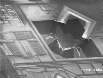
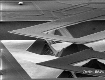
Examples of catastrophic faults for the device:
SEM images of a broken beam and a non-released one. (Credit: LIRMM)
More information about this study can be found in the following papers:
- A. Chaehoi, Y. Bertrand, L. Latorre, P. Nouet ; “Improving the efficiency of the Oscillation-Based Test Methodology for Parametric Faults” ; LATW’03: 4th IEEE Latin-American Test Workshop, Natal (Brazil) ; February 16-19, 2003, pp. 234-237
- A. Chaehoi, L. Latorre, F. Azaï s, P. Nouet ; “Use of a Statistical Approach for Efficient Implementation of Oscillation Based Test Strategy” ; IMSTW’03: 9th International Mixed-Signal Testing Workshop, Sevilla (Spain), June 25-27, 2003, pp. 99-103.
Design of CMOS monolithic FSBM inertial sensors
After my year of Post Graduate study, I have been offered to continue to work for the same group on the design of micro-sensors. This is when I really get excited by Research. After all the years spent on the benches of the university, finally I was about to work on something very exciting, a subject that I have chosen and defined. Furthermore, the study would be in collaboration with an Italian university which implied to spend a few couple of months in Sicily. What more could I ask for?
I have done my PhD study under a co-supervision agreement between LIRMM, a microelectronics laboratory in Montpellier - France, and a Sicilian laboratory in Italy, DIEES. The aim of my research study was to investigate the potential that CMOS monolithic process could offer in terms of inertial sensing device.
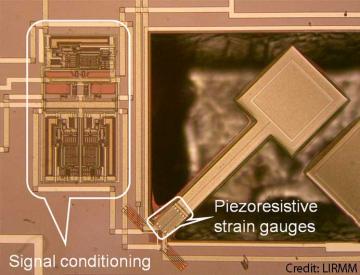
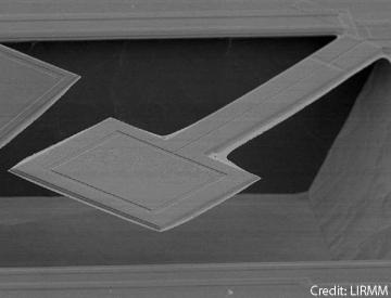
According to designer requirements several etching masks can be superimposed to leave the silicon bulk uncovered at the end of the standard CMOS process. Then, the post-process operates as an anisotropic silicon etching that uses the various oxide layers as self-aligned masks. <100> substrate planes can then be etched leaving the <111> planes of silicon substrate unaltered. In that way, suspended structures can be obtained as a heterogeneous stacking of various materials. Anisotropic wet etching of CMOS bulk from the front side is the cheapest way to achieve suspended structures leading to monolithic CMOS MEMS. However, the obtained structures do not offer important seismic mass while mechanical deformations are sensed using standard non-optimized polysilicon strain gauges. For these reasons, front-side bulk micromachining (FSBM) is not considered for inertial applications. During my study I have demonstrated that despite non optimized seismic mass and gauge factor, low-cost CMOS suspended structures can be used for inertial sensing. The piezoresistive CMOS beams exhibit a low noise level, thus enabling reasonable resolution. Moreover, in the context of fully monolithic fabrication approach, electronic circuitry can be designed to improve the sensor performance. The proposed device is a simple "T-shaped" cantilever beam. The acceleration (out-of-plane) is measured by means of two embedded strain gauges that convert the vertical displacement of the mechanical structure into resistance variations. The piezoresitive strain gauges are arranged in a Wheatstone bridge and connected to a dedicated on-chip instrument amplifier.
|
|
|
Pictures of the proposed sensor and its associated CMOS electronic circuit.
Source: A.Chaehoi – Eurosensors’04
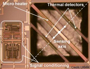
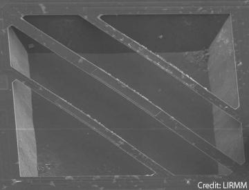
This piezoresistive device was designed to measure only out-of-plane acceleration. Using the same CMOS FSBM technology, I have also designed an in-plane axis accelerometer based on thermal convection effect. A heating resistor flanked by two temperature detectors is suspended over a cavity. The symmetric temperature profile created by the heater become asymmetric with the acceleration, this temperature variation is converted into a resistance variation on the thermal polysilicon detectors. The detectors are here again arranged in a Wheatstone bridge and connected to an on-chip instrument amplifier.
|
|
|
Pictures of the thermal accelerometer and its associated CMOS electronic circuit.
Source: A.Chaehoi – Eurosensors’05, A.Chaehoi – Sensors&Actuators’06
|
|
| (Video : Better compatibility with Internet Explorer) | |
During my PhD study I have demonstrated that the self-aligned wet-etching of CMOS bulk from the front side (FSBM) – the cheapest way to manufacture suspended structures and so monolithic microsystems – can be used to manufacture low-cost inertial sensors.
More information about this study can be found in the following selection of papers:
- A. Chaehoi, L.Latorre, F.Mailly, P.Nouet ; “Experimental and Finite –Element Study of Convective Accelerometer on CMOS” ; Sensors and Actuators A (132) 2006, pp 78-84
- A, Chaehoi, N. Dumas, F. Mailly, L. Latorre, P. Nouet ; “Absolute Pitch Roll and Yaw Measurement on CMOS” ; IEEE Sensors’05, Irvine (California) ; October 31-November 03, 2005, pp.133-136
- A. Chaehoi, L.Latorre, F.Mailly, P.Nouet ; “Experimental and Finite –Element Study of Convective Accelerometer on CMOS” ; Eurosensors’05, Barcelona (Spain) ; September 11-14, 2005, mp. 23
- A. Chaehoi, L. Latorre, P. Nouet ; “Design of CMOS Cantilevers for Inertial Sensing” ; Euspen 2005: 5th international conference and 7th annual general meeting of the European Society for Precision Engineering and Nanotechnology ; Montpellier (France) ; May 8-11 2005, pp341-344
- A. Chaehoi, L. Latorre, P. Nouet ; “A CMOS MEMS Accelerometer with Bulk Micromachining” ; Eurosensors’04: 18th European Conference on Solid-State Transducers, Rome (Italy) ; January 28-30, 2004, pp.287-292
Design of CMOS monolithic sensors on SOI
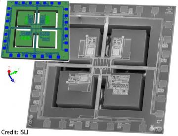
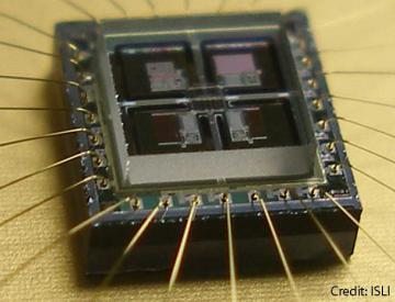
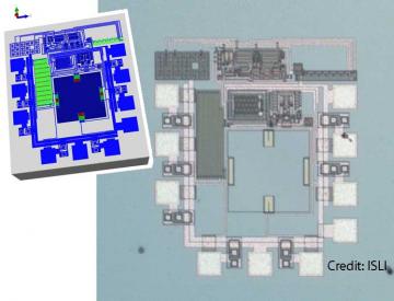
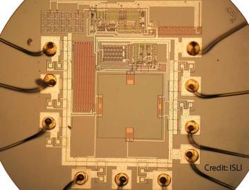
I have joined the Institute for System Level Integration (ISLI) after my PhD. On top of various different academic research projects, I have been assigned to support and help one of our industrial partners in the development and integration of a CMOS-SOI MEMS-compatible process. The aim was to transfer an existing CMOS electronics process into a process on which we could develop monolithically integrated MEMS sensors. I have then design on the developed process two different sensors: a fully integrated 3-axis piezoresistive accelerometer and a pressure sensor. Zero-level packaging was achieved using anodic bonding of a pyrex wafer on the back-side and a BCB-based bonding approach to attach another pyrex wafer to the front-side.
|
|
|
Pictures of the monolithic CMOS 3-axis accelerometer and pressure sensor.
Source: A.Chaehoi – Microtech’10, A.Chaehoi – Sensors & Transducers Journal’11..
|
|
|
More information about this study can be found in the following selection papers:
- A. Chaehoi, M. Begbie, D. Weiland, D. O’Connell, S. Ray; “ Piezoresistive Sensors Development Using Monolithic CMOS MEMS Technology ” , Sensors & Transducers journal (ISSN 1726-5479), Vol.11, Special Issue, April 2011, pp.42-51.
- A. Chaehoi, D. O’Connell, D. Weiland, S. Buckshaw, M. Begbie; “Monolithc CMOS MEMS technology development: A piezoresistive-sensors case study” ; Microtech’10, Anaheim, California, 21st – 25th June, 2010, Vol.2 pp. 284-287.
- A. Chaehoi, D. Weiland, R. Adamson, M. Begbie, C. Lowrie, M. Desmulliez, G. Brown, L. Li, D. Uttamchandani; “On the design of an integrated monolithic 3-axis piezoresistive accelerometer on SOI” ; ESSDERC 2008, Edinburgh, September 2008.
Design and modelling of microactuators for micro-optical applications
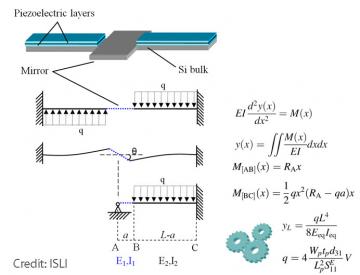
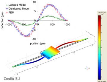
I am involved in a collaborative research venture: the Scottish Consortium in Integrated Micro-Photonic System (SCIMPS ) where my work concerns the development and the modelling of microactutors for optical applications. I closely worked with a university research group which developed AlN piezoelectric films. AlN being a very good material candidate for the development of integrated MEMS (lead-free, CMOS-compatible, spontaneous polarization, etc.), I proposed to use this material developed by one of our University partner to develop actuators that could be used within the SCIMPS consortium. The proposed devices range from optical micro-scanner to energy-scavenger to integrated ultrasonic cell-imager.
|
|
|
Examples of model development of a piezoelectric micro-scanner.
Source: A.Chaehoi – Journal of Microsystem Technologies ’08, A.Chaehoi – DTIP’07.
More information about this study can be found in the following papers:
- A. Chaehoi, M. Begbie; “Study of a piezoelectric multimorph based micro-scanner” ; Journal of Microsystem Technologies, Vol. 14, No. 7, July 2008, pp. 963-969
- A. Chaehoi, M. Begbie, D. Cornez, K. Kirk; “ Modeling of a piezoelectric micro-scanner” ; Design Test Integration and Packaging of MEMS / MOEMS DTIP’07, Stresa, Italy, April 25-27, pp.151-155
Piezoelectric AlN thin film MEMS structures development
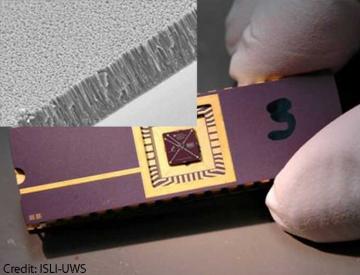
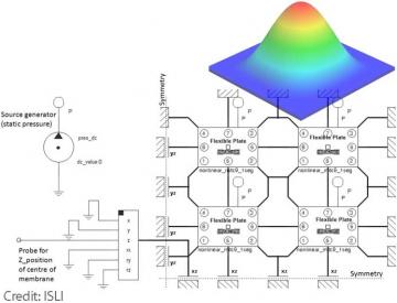
One of my research collaboration and activity is about the development of MEMS structures for the characterization and the electrical and mechanical study of AlN thin-film based MEMS. MEMS device structures for integrated microelectronic systems incorporating piezoelectric thin films frequently involve layers of active material deposited onto membranes or beams. In these structures, intrinsic stress in the piezoelectric layer will affect the behaviour of the device. Experimental work and modelling were used to investigate flexural modes of the structures and to assess the use of system-level modelling for these AlN based structures.
|
|
|
Picture of a packaged membrane device on top of which the AlN film is deposited and example of model development.
Source: K.Kirk, A.Chaehoi – Euromat ’09; D.Cornez, A.Chaehoi – Electroceramics’08.
More information about this study can be found in the following papers:
- K. Kirk, A. Chaehoi, D. Cornez, M. Begbie, D. Hutson; “ Characterisation and system-level simulation of piezoelectric aluminium nitride thin film MEMS structures” ; EuroMat’09, Glasgow, UK, 7th - 10th September 2009
- D. Cornez, K. Kirk, A. Chaehoi, M. Begbie; “ Electrical and optical characterisation of aluminium nitride piezoelectric films on silicon nitride membranes” ; Electroceramics XI, Manchester, 31th August - 4th September 2008.
Multiple-output MEMS DC/DC converter
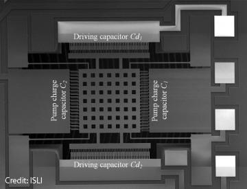
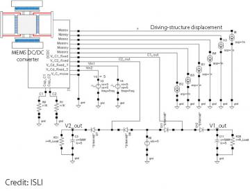
One exciting MEMS device I have been recently working on is a single-input multi-output MEMS DC/DC converter. DC/DC converters are widely used in consumer electronic devices where usually a single power source is available while the electronic board of the device requires different voltage levels in order to power-up different block functions. This study is about the design of a MEMS single-input multi-output voltage level shifter. The low-voltage to high-voltage conversion is based on the electrostatic transduction of variable capacitors built using interdigitated comb fingers. In this study I presented the co-design and co-simulation of the whole system (the MEMS device and its dedicated charge-pump-circuit) in a single EDA environment through MEMS+ [a Coventorware® tool that allows the co-simulation of MEMS and electronics in the Cadence Analog Design Environment (Virtuoso)]. I have developed analytical, FEM and MEMS+ models of the multi-output DC-DC converter and show that all the developed models converge towards the experimental results.
|
|
|
SEM picture of the dual-output MEMS DC/DC converter and schematic view of the whole DC/DC converter system in Virtuoso.
Source: A.Chaehoi – Smart System Integration ’11
More information about this study can be found in the following paper:
- A.Chaehoi,M. Begbie, D. Weiland, “Multiple-output MEMS DC-DC converter” , DTIP’11,Aix-en-Provence, France, 11-13 May 2011.
- A. Chaehoi, D. Weiland, M.Begbie, S. Scherner, “MEMS DC-DC converter: A detailed CMOS mechanicalco-simulation” , Smart System Integration, Dresden, Germany, 22-23 March.
